 Unveiling Its Core Strategy to Capture the Hundred-Billion Optoelectronic Integration Market
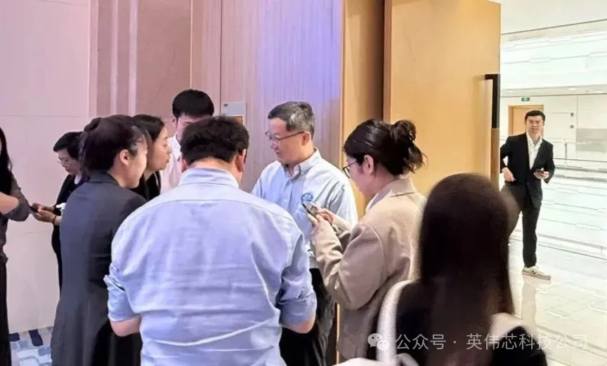
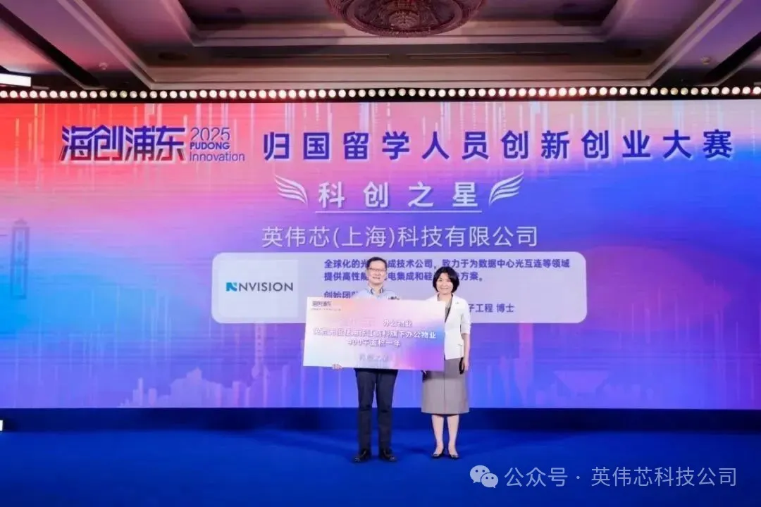
On May 15, the "Haichuang Pudong" competition concluded. Nvision won the top prize, the "Technology Innovation Star" award, thanks to its independently developed cutting-edge "Optoelectronic Integration Platform." Right after stepping off the stage, founder Nie Hui was swarmed by investors, exchanging contacts and extending invitations.
What kind of technology could attract investor interest immediatly? And how to seize the key breakthrough points in the emerging hundred-billion-RMB market of next-generation optoelectronic integration market?
Recently, Zhangtongshe visited Nvision (Shanghai) Technology Co., Ltd. for an exclusive interview with Nie Hui, delving into the core barriers of optoelectronic integration and unveiling the company’s strategic path to capturing this high-stakes market.

Thirty Years of Dedication to Optoelectronic Devices
Leading Intel’s Cutting-Edge Silicon Photonics Projects
To understand Nvision’s breakthrough path, one must begin with its founder, Nie Hui—his story is itself a history of deep commitment to the field of optoelectronic devices.
In the late 1980s, Nie Hui was admitted from Yangzhou High School to the University of Science and Technology of China (USTC), where he majored in physics. Immersed in the intense atmosphere of USTC’s “study-abroad preparatory program,” he set his sights on pursuing education overseas as early as his sophomore year. In 1993, he went to the United States to earn a Ph.D. in electronic engineering.
The foreshadowing of his destiny was quietly set—his doctoral research focused on high-performance photodetectors. His advisor hailed from Bell Labs, regarded as a “holy land” for optoelectronic devices. After graduation, Nie Hui naturally transitioned into joining the lab, officially embarking on his deeply dedicated journey in the field of optoelectronic devices.
As an R&D engineer, Nie Hui’s eight-year experience at Lucent Bell Labs shaped his initial understanding of industry cycles. He witnessed the frenzy and decline of the first internet revolution: the optoelectronics division expanded from 300 to 2,500 employees, with daily revenue exceeding US$2 million at its peak and an investment bank valuation of US$70 billion. Yet after the dot-com bubble burst in 2000, the team shrunk to 150 people, and performance plummeted by over twentyfold.
“Our technology kept improving, so why did our performance keep worsening?” This question led to an epiphany: technology detached from market demand would ultimately become a castle in the air. “To look beyond” became his strongest urge at that moment.
Driven by this reflection, he decisively stepped out of his comfort zone in pure technical R&D: first transitioning into a product manager to closely follow the entire process from R&D to sales, then joining a startup as a technical expert and CTO, where he participated in cross-border acquisitions and gained deep insight into corporate operations. Nearly a decade of hands-on experience gave him a comprehensive understanding of the market dynamics of optoelectronic devices, as well as product development, operations, and marketing.
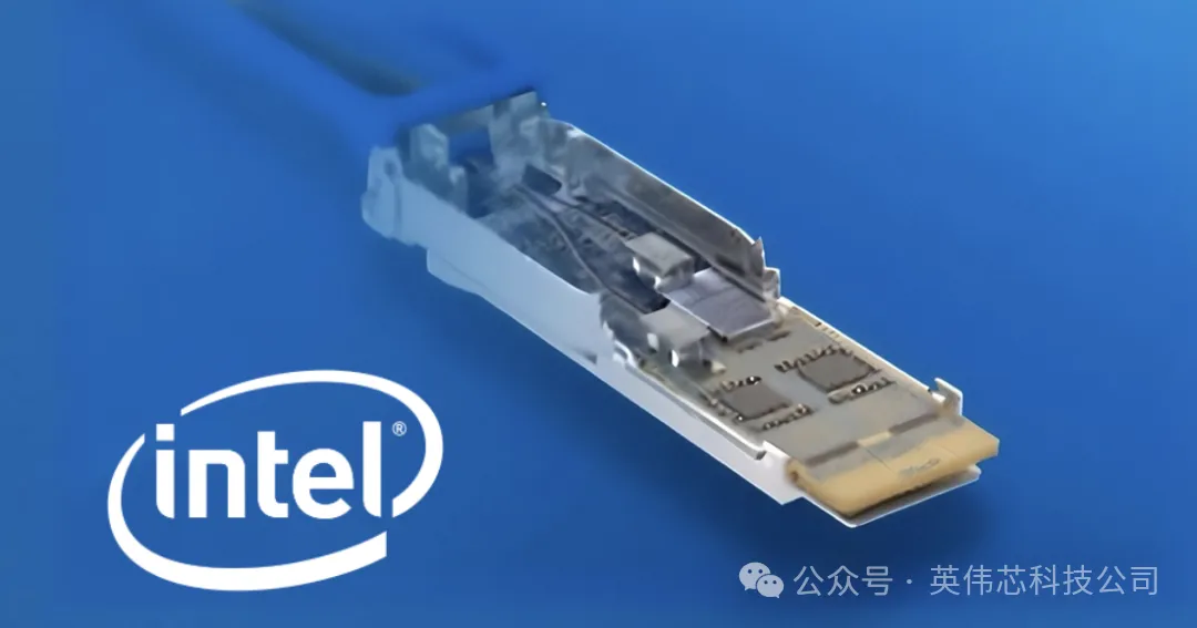
In 2015, Nie Hui was invited to join Intel to lead its cutting-edge silicon photonics products. This became a critical leap in his career. At a time when silicon photonics was still largely unknown in China, he was already immersed in developing the world’s first low-cost, mass-producible silicon photonics product. This project, which originated in Intel Labs and went through nearly ten years of R&D, achieved the leap from 1 to 100 under Nie Hui and his team’s leadership. Their core breakthrough was transforming discrete optoelectronic components into a platform capable of mass production via CMOS semiconductor processes.
To date, this platform has mass-produced and shipped over 8 million fully integrated silicon photonic chips, with reliability far exceeding that of traditional discrete laser devices. At the very place where Moore’s Law was proposed and flourished, Nie Hui came to a profound realization: photonics could also evolve in accordance with Moore’s Law.
In 2019, Nie Hui returned to China and joined a leading lidar startup, establishing its optoelectronic device department from scratch. At the time, lidar systems relied on discrete laser and detector components, which were manually assembled and often cost over RMB 100,000 per unit. Guided by the logic of Moore’s Law, Nie Hui led his team to develop a new technology from the ground up—one that was initially overlooked by the market but held strong potential for iteration. He also firmly committed to partnering with then-nascent domestic supply chains to advance the localization of high-end core components. Within a few years, the team not only reduced lidar costs to less than one-tenth of the original but also improved performance by more than tenfold.
This validation of Moore’s Law further convinced Nie Hui that the breakthrough in optoelectronic devices must follow the path of “photonic-electronic integration + CMOS processes”—which could very well be the key to overcoming bottlenecks in the optical interconnect industry.
In 2024, fueled by this conviction, he founded Nvision. The core team quickly brought together seasoned experts from Intel, leading lidar companies, and AI tech firms. Members have successfully achieved breakthroughs in key technologies such as 100G silicon photonic chips, high-power vertical-cavity surface-emitting lasers (VCSELs), high-sensitivity single-photon avalanche diodes (SPADs), and highly integrated lidar chips from scratch, and have passed the market test of large-scale mass production and delivery. A golden combination of “technical depth + industrial execution” had officially formed.
Years of in-depth exploration at Bell Labs, the rigor of high-volume manufacturing at Intel, and the performance-cost revolution at the lidar company—every step of this journey now converges toward a single goal: to write a new chapter of Moore’s Law for next-generation photonic-electronic integration.
Nvision is committed to tackling the most persistent challenges that have long plagued the industry.

Targeting the Next Pain Point in AI Computing Clusters
Enabling Optical Interconnects to Follow Moore’s Law
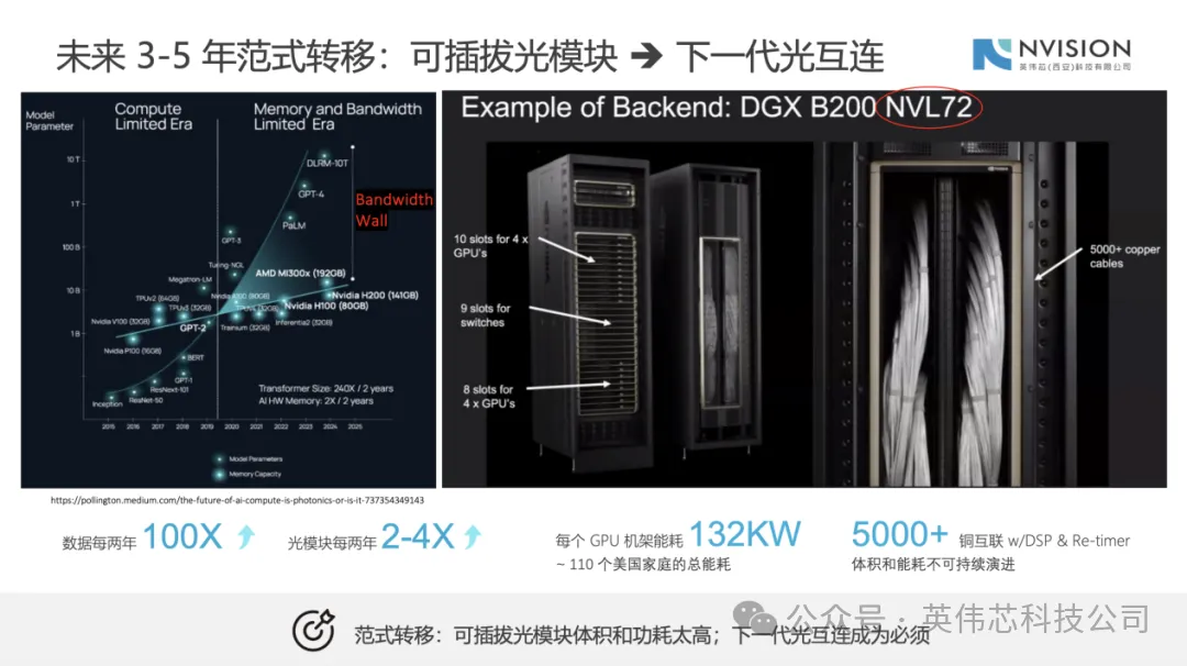
Nvision’s technological direction is based on a simple yet critical observation: while the growth of computing power has surpassed the predictions of traditional Moore’s Law, data transmission (interconnect) capabilities have failed to keep pace.
Take, for example, large-scale GPU clusters (“thousands of cards”). Their parallel architecture requires massive real-time data exchange, yet traditional copper cables and optical modules offer limited single-channel capacity, failing to meet these high demands. As a result, systems are forced to rely on over 5,000 copper cables or a similarly vast number of optical modules to handle parallel computation and data transfer. This not only causes energy consumption per GPU rack to sour (132 kW ≈ the energy usage of about 110 U.S. households), but the complex cabling also significantly raises cooling and power supply costs, trapping the system in a vicious cycle where “bigger scale means higher energy consumption.”
The conflict between the exponential growth in computing demands and the linear improvement in traditional optical modules has created an unprecedented need for a “paradigm shift” in technology.
The solution proposed by Nie Hui’s team is Optical I/O (OIO) technology. By leveraging wafer-level heterogeneous integration, Nvision combines optoelectronic materials with silicon-based wafers and utilizes CMOS processes to achieve mass production—for the first time enabling optoelectronic devices to improve in performance and integration in accordance with Moore’s Law.
“Simply put, it’s about tightly bonding optoelectronic devices onto silicon,” explained Nie Hui. While optoelectronics have not yet kept pace with Moore’s Law, silicon has long undergone upgrades in a market worth hundreds of billions. Applying silicon’s “Moore’s Law” principles to optoelectronic devices can transform traditionally “handcrafted” optical modules into “chip-level” products. In his view, only by introducing Moore’s Law can the challenges of bandwidth, power consumption, and cost in optical interconnects be truly resolved.
Guided by this approach, Nvision’s product efficiency can be described as “overwhelmingly superior”—delivering a 10x increase in bandwidth density, a 90% reduction in energy consumption, latency compressed to 5ns, and significantly lower costs. This fully meets the core demands of optical interconnects: high density, low power, and low cost.
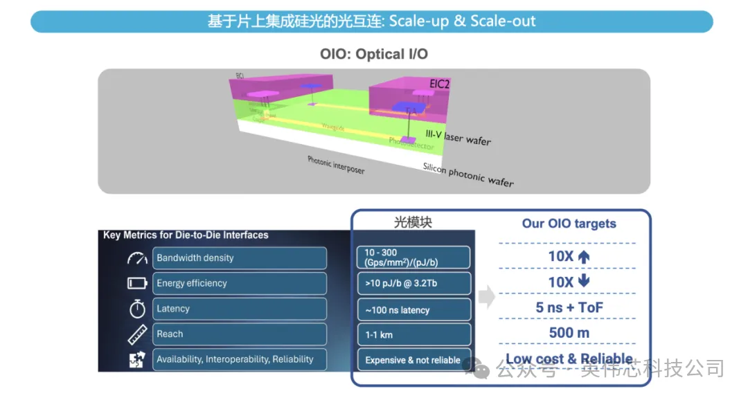
This technology holds exceptional value for AI data centers. In a well-known solution, each GPU typically requires 18 optical modules to enable high-performance cluster interconnection. Nvision’s OIO solution dramatically reduces this ratio while supporting high-density signal transmission over distances of up to 500 meters, perfectly meeting the “Scale-up & Scale-out” demands of AI clusters. More importantly, it can not only replace copper cables and traditional optical modules but also integrate with advanced packaging technologies for CPUs and GPUs, serving as a “superhighway” for AI computing power.
In terms of product strategy, Nvision has built a tiered product matrix: near-term focus on PCIe optical interconnect modules, with mass production expected as early as next year; medium-term development of Ethernet optical engines targeting short- to mid-reach transmission in servers and switches; and long-term commitment to wafer-level OIO to fundamentally redefine data center interconnect architecture. This combination of fast commercial wins and long-term R&D ensures a structured approach to market entry while targeting a multi-billion-dollar market opportunity.
3.2T 2.5D-Packaged CPO,External Laser Source
This technological direction quickly gained recognition from investors. In April, Nvision secured over ten-million RMB in angel funding from CAS Star. The investor stated that itConfidence in the Nvision team stems from its extensive experience in III-V photonic chips and silicon photonics, as well as its proven execution in optoelectronic integration. Furthermore, Nvision is poised to form strong upstream and downstream synergies with CAS Star’s ecosystem in the optoelectronics semiconductor industry, demonstrating significant potential for expanded applications.
Yet this capital injection is only the prologue to a broader revolution in optical interconnection.

Winning Star in Zhangjiang
Breaking Through in the Trillion-Dollar Photonics Arena
Nvision’s growth momentum continues to accelerate, garnering not only capital investment but also recognition from both industry and local government. At the “Haichuang Pudong” awards ceremony, Li Hui, Deputy District Governor of Pudong New Area, presented Nvision with the “Sci-Tech Innovation Star” award. The company will receive high-quality space support in Zhangjiang, providing tangible bolstering for the team’s R&D and operations.
Behind this recognition lies the vast potential of the photonics industry. According to data from the China Academy of Information and Communications Technology (CAICT), the global photonics industry reached USD 920 billion in 2023 and is projected to grow to USD 1.2 trillion by 2027. Zooming in on the optical interconnect segment, the global market is expected to grow at a compound annual growth rate of 13.15% from 2024 to 2029, reaching over USD 31.8 billion (RMB 228.4 billion) by 2029.
Nie Hui admitted that Nvision's focus on the optical interconnect is first and foremost due to the segment’s promising prospects and large market size. More crucially, however, the company’s unique mastery of wafer-level heterogeneous integration technology presents a high barrier to entry. In addition, the absence of dominant players in the field has opened a valuable window of opportunity. Speaking on returning to China to start a business, he offers a sharp insight: “Based on my years of experience and observation both domestically and internationally, I find that the average skill level of engineers in China is higher, the pace of technological evolution is faster, and the current ecosystem is highly conducive to entrepreneurship.”
Rooting the core team in Zhangjiang was a strategic decision informed by the area’s industrial ecosystem. As a high-level tech talent in Shanghai, Nie Hui is well aware of Zhangjiang’s unique strengths in semiconductors—from rare silicon photonics foundry lines and packaging-test chains to integrated circuit industry funds and AI computing scenarios. Zhangjiang offers startups end-to-end support “from tape-out to customer engagement.” Since entering a Zhangjiang incubator, Nvision has rapidly achieved key milestones, gaining not only space and policy support but also directly connecting with industrial capital partners like CAS STAR through park-sponsored salons, engaging with AI companies and teams, and reaching potential customers and business partners.
Looking ahead, Nie Hui is confident: “We believe the AI era is not a bubble. Much like revolutionary industrial shifts brought by the steam engine and the computer, AI will genuinely and profoundly transform society and people's lives.”
As technological breakthroughs, policy tailwinds, a fertile ecosystem, and market channels converge, a photon buried in silicon-based soil is quietly rewriting the energy trajectory of the computing world—redrawing the competitive landscape of the global optical interconnection industry.


